This final year project, a 0.5KVA solar based inverter design, was carried out by Ifeanyichukwu Opara, a student of Covenant University Ottah, from the department of Electrical Engineering. This is a joint collaboration between him and Smartech to design a 0.5KVA Solar Based.
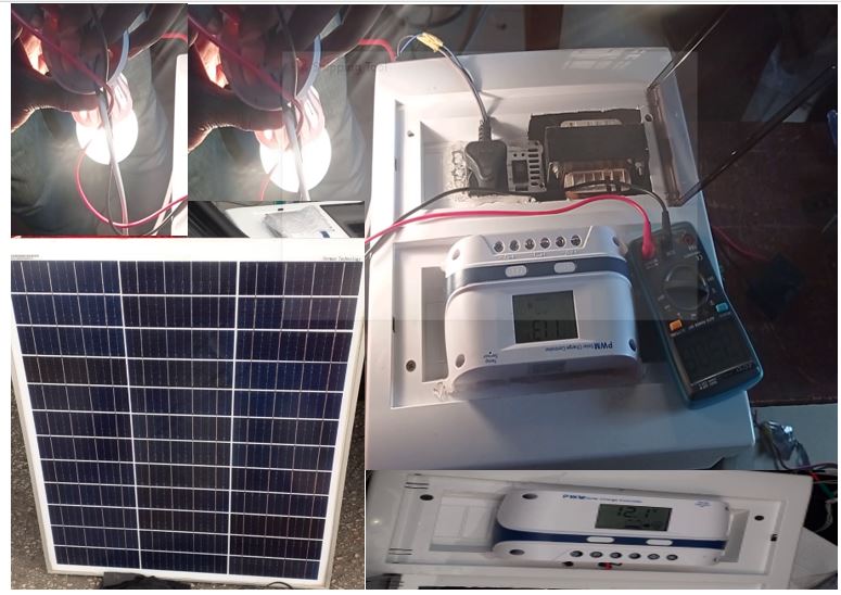
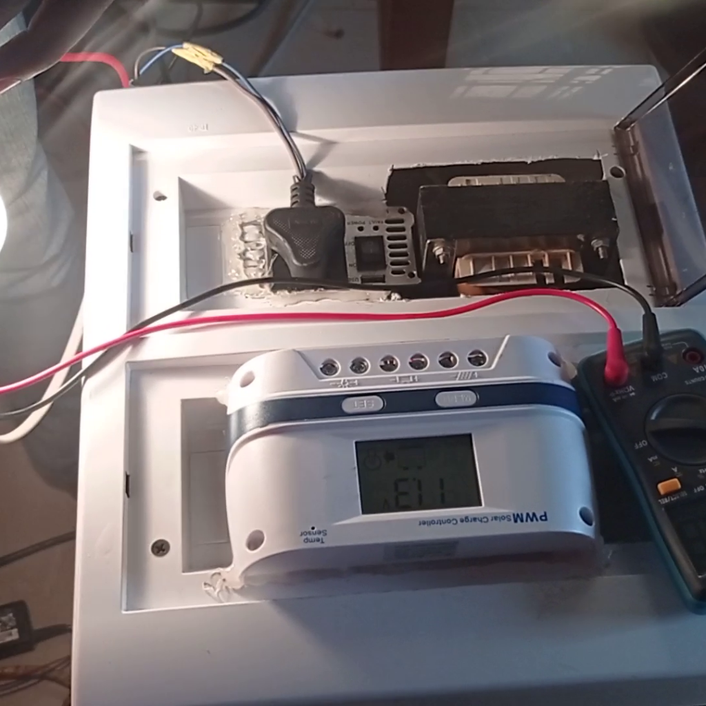
This project design is a pure sine wave solar based inverter that uses a 100W panel to recharge a 12V Battery through a PWM charge controller as shown here. The charge controller would display that the battery is connected. The battery voltage too is displayed.

Materials and Components Needed for this Project
- Print Circuit Board (PCB) of the inverter
- 12V relay…2 pieces
- N-Channel MOSFETs….8 pieces
- 100k Potentionmeter…2 pieces
CONTACT US HERE FOR FULL KIT OF THIS PROJECT
The Inverter Calculations
Determination of the Number of MOSFETs Required
Since the input voltage is taken from the battery which supplies voltage that could range from 12v to 48v to the input side of the transformer, then; the least voltage level was selected for the analysis to enable calculate using maximum current possible.
Input voltage = 12V
MOSFET Type: IRF250N; Id = 50A, Vds = 200V
Required output power = 1500VA
The maximum drain current of the MOSFET is 50A at 100°C but it is difficult to keep the MOSFET at this temperature during high power operation, hence the need to de-rate. Choosing the maximum drain current for each MOSFET during maximum power operation to be 30A; Maximum drain current for each MOSFET — 30A. The required current from the input side of the transformer for the power output to be at 1500 VA was calculated using:
Current = power/voltage
Current = 1500/12 = 125A
Number of MOSFET = Maximum current / MOSFET drain current
=125/30
=4.166 = 4 MOSFETs per branch
A push-pull circuit has 2 branches, therefore: total number of MOSFET= 2×4 = 8 MOSFETs.
Heat Sink Selection
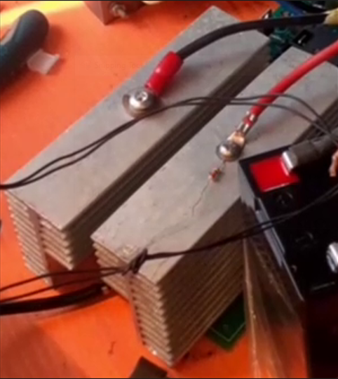
The use of heat sink in this 0.5KVA solar based inverter project design was introduced in order to keep the temperature of the semiconductor below 125 C. When power MOSFETs are delivering very high power due to the connected output, they operate at a very high temperature (maximum temperature is 150C). There arises a need to keep the temperature below the maximum operating temperature. Hence, the need for a material capable of being called a heat sink, which possesses a thermal conductivity to keep the temperature at a bearable level for the components. A heat sink is a component or assembly that transfers heat generated within a solid material to fluid medium, such as air or liquid. Examples of heat sinks are heat exchangers used in refrigeration and air conditioning systems. The most common heat sink material is Aluminium. Chemically pure Aluminium is not used in the construction of heat sink, but rather Aluminium alloy. This has a very high thermal conductivity, soft to work on and light in weight. Also, copper can be used for this purpose since it has around twice the conductivity of Aluminium, but heavier and more expensive than Aluminium.
Transformer Selection
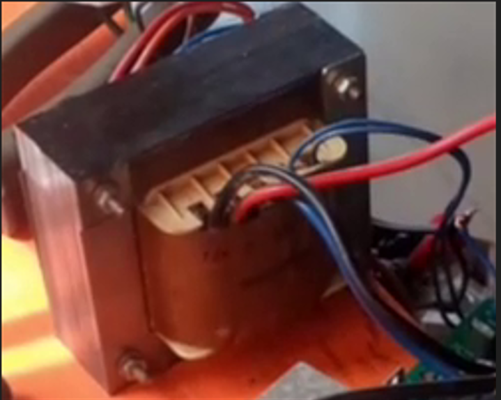
The design inputs of the transformer at the start of designing are listed below:
- Secondary Voltage = 230 Volts,
- Secondary Voltage = 7 Amps
- Primary Current (Output Current) = 50 Amps.
- Primary Voltage (Output Voltage) = 10-0-10 volts
- Output Frequency = 50 Hz
Calculating Inverter Transformer Voltage, Current, Number of Turns
Calculating Turns per Volt (TPV) = 1/ (4.44 x 10⁻⁴ frequency x core area x flux density)
TPV = 1 / (4.44 × 10–4 ×18 × 1.3 × 50) = 1.96 turn per volt.
Therefore the Number of Turns for the Secondary winding is calculated as = 1.96 × 230 = 450
Secondary Winding Area becomes = 450 / 137 = 3.27 sq.cm.
Calculating Primary Number of Turns = 1.04 (1.96 × 24) = 49. The value 1.04 is included to ensure that a few extra turns are added to the total, to compensate for the winding losses.
The reason for using 10V-0-10V as secondary, is enable maintain 230V output when the battery level reduce to 10v during the inverting process.
For 10V = 10 x 1.5 = 15 turns.
The transformer winding wire sizes are selected from the standard wire Guage selection table.
Solar Charge Controller Sizing
The solar charge controller is typically rated against Amperage and Voltage capacities. Select the solar charge controller to match the voltage of PV array and batteries and then identify which type of solar charge controller is right for your application. Make sure that solar charge controller has enough capacity to handle the current from PV array.

For the series charge controller type, the sizing of controller depends on the total PV input current which is delivered to the controller and also depends on PV panel configuration (series or parallel configuration). According to standard practice, the sizing of solar charge controller is to take the short circuit current (Isc) of the PV array, and multiply it by 1.3.
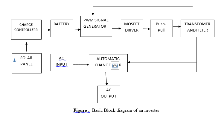
The block diagram below shows various parts of the project that will be addressed. The signal generator is simply the SG3524 PWM IC. It generates both the PWM and square wave signals needed in controlling the MOSFET drivers. The signals from the drivers are then used to drive the four N-channel MOSFETs in the Push-Pull configuration. The output signal from the Push-Pull is then sent through a step-up transformer and a low-pass LC filter so that the final output is a pure sine wave at 50Hz frequency.
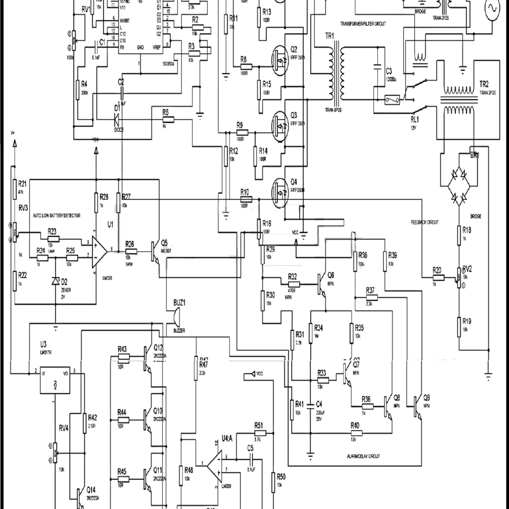
The 0.5VA Solar Based Inverter Circuit Diagram
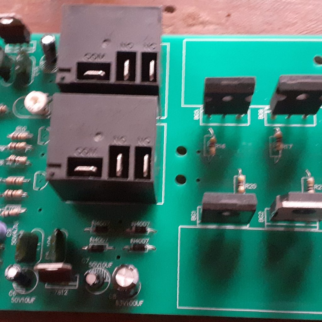
PCB and Circuit Assembly

The 0.5kVA solar powered inverter circuit diagram is manufactured on a PCB. Once the PCB is out of production as shown above, the assembly of the components begin.
Read More
- Anti-Theft and Burglar System with SMS Notification
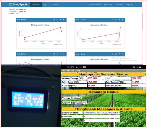
- How to build a Smart Hydroponics IoT Project
- How To Generate Electricity using foot-steps with backup charging station (Piezoelectric generator) Project
Assembly of the components started like this, we placed all the needed components on the PCB and soldered them onto the PCB. These relays here are used to switch between inverted AC voltage output and AC mains output.
Testing the Assembly
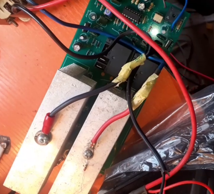
The heatsinks are important and had to be connected because without them, the heat dissipated by the N-Channel MOSFETs would eventually damage the MOSFETs themselves. Also, it is a source to drain current. When the heatsinks are connected, we can quickly run a test to see if things are going in the right direction. All connections are terminated accordingly and a miniature 12V DC battery is used for this test.
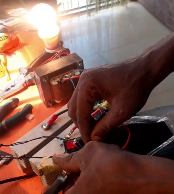
Please remember to wear an insulation glove while dealing with this design at this stage. connecting the control part of the inverter circuit to the battery. We can see that the AC light bulb comes on.
Calibrating of the Solar Based Inverter Design
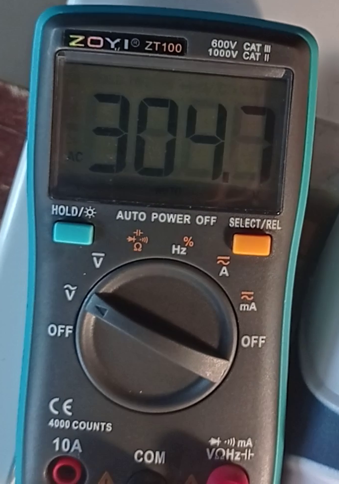
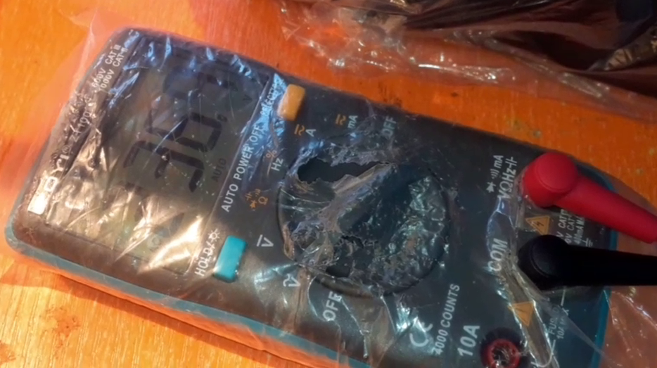
The amplitude of the voltage is also quite high hence the light intensity of the AC light bulb is bright. There is the need to calibrate the inverter from 330V to 220-250V range. This is done by adjusting the potentiometers on the inverter board. The voltmeter reads the AC voltage of the inverter output when it is turned on. We can see it go from 0V to 235V AC. This is a good output AC voltage.
Casing the Solar Based Inverter Design
We start encasing the design in a plastic casing. This plastic box was spacious enough to contain the design and also has opening and ports for AC and DC output. The system design can power both AC and DC loads.
Conclusion
This project, design and construction of 0.5KVA solar based inverter has been carried out successfully. It has been tested and found to be working. You can follow the steps here, order for the complete kits which includes the PCB design and the components to get you started on the project work. Let us know what you think about this project in the comment section below. Thank you.